The goal of this term project is to implement a 16-bit Floating Point Adder, utilizing IEEE’s
Standard 754 Floating Point Number Representation. This calculator was created on an Intel Altera
FPGA. More specifically, the Terasic Technologies MAX DE-10 FPGA was used. This project is the
culmination of the Digital Logic courses I’ve taken. In addition to providing a greater
understanding of general digital logic concepts, this project allowed for much more practice
with FPGAs and the SystemVerilog programming language. A short demonstration of the resulting
calculator can be found below:
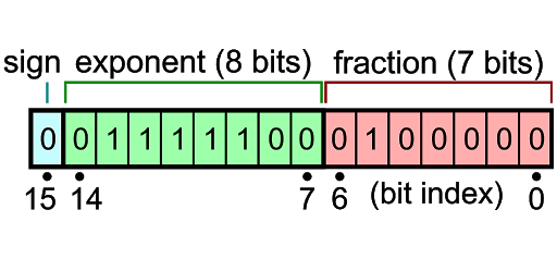
As mentioned, the floating point calculator follows IEEE’s floating point standards, meaning
the resulting output from these calculations follow the below format, and calculations follow the
recommended process for adding floating point numbers. Below is a reference for the format of
these floating point numbers, including ranges for the sign, exponent, and mantissa/fraction bits:

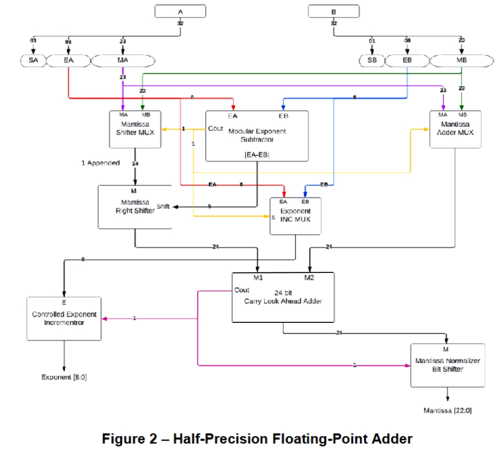
The calculator is implemented in SystemVerilog on an Altera FPGA, following the data flow from
the below diagram. This diagram outlines the general process for which our floating point numbers
are summed together. Each block on the diagram describes a different implemented module/component
of the calculator. Each of these components accomplish various different processes in the
addition’s data flow. Most of these components are separated into their own SystemVerilog
module/file, and a list of these components can also be found below:

Exponent Subtractor (ExponentSubtractorFiveBit.sv)
Modular Multiplexer (3 Instances) (modularMux.sv)
Right Barrel Shifter (2 Instances) (ElevenBitRightShifter.sv)
Group Carry Look-Ahead Adder (TwelveBitGCLA.sv)
Controlled Incrementer (FiveBitIncrementer.sv)
LCD Display Configurator (LCD_Board_Test_LCD.sv)
Keypad Configurator (InputUnit.sv and clock_div.sv)
When all of these components and their dependencies are combined and instantiated, the floating
point calculator is complete. Demonstrations for the functioning calculator are shown in the above
video, and the chosen test case are found below:
Test Case 1: 3.75 + 5.125 = 8.875
| Decimal Representation | Hex Representation | Binary Representation | |
|---|---|---|---|
| Input A | 3.75 | 0x4380 | 0 10000 1110000000 |
| Input B | 5.125 | 0x4520 | 0 10001 0100100000 |
| Result R | 8.875 | N/A | 0 10010 0001110000 |
Test Case 1: 9.5 + 0.5625 = 10.0625
| Decimal Representation | Hex Representation | Binary Representation | |
|---|---|---|---|
| Input A | 9.5 | 0x48C0 | 0 10010 0011000000 |
| Input B | 0.5625 | 0x3880 | 0 01110 0010000000 |
| Result R | 10.0625 | N/A | 0 10010 0100001000 |
This section of the report will delve into my implementation of the coding/software portion of
the project. As described above, most of the calculator’s components are separated into their own
module files. Below is a download link for the zipped folder, containing all of the SystemVerilog
files used in the calculator’s implementation. Utilized FPGA pin declarations are not included.
Please feel free to read through the relevant files as necessary. These files can also be found
in my GitHub:
David Denny Zipped Altera FPGA Project Folder
Below are just a couple more notes for some files that deserve some additional explanation:
- The calculator component instantiations can be found in LCD_Board_Test_LCD.sv. In this way,
LCD_Board_Test_LCD.sv can be considered the top module for this project.
- Input values are registered and obtained from using a connected 4x4 keypad array in a hexadecimal
configuration. The process for which these input values are obtained can be viewed in InputUnit.sv
and clock_div.sv.
- Additionally, the outputted values from the calculator are displayed on a connected LCD display
using included libraries. Instantiations of this functionality can be found in
LCD_Board_Test_LCD.sv, but the library files themselves are not included. This functionality
can also be seen in the video demonstration.
- Lastly, condition code logic for Underflow and Overflow are implemented. Those signals simply
drive two LEDs on the FPGA.
Overall, this lab is the culmination of many Digital Logic concepts studied and practiced
throughout my relevant courses. In its totality, it is a very in-depth and complicated project,
and has enabled me to practice writing and understanding SystemVerilog, in addition to the
concepts of Digital Logic in general.