The project includes the creation of a simplified RISC-V processor using an AMD Xilinx Blackboard FPGA, hereby
referred to as the Blackboard. The Blackboard allows for the creation of this CPU, using the SystemVerilog
programming language. The goal of this project is to implement a RISC-V processor with a five stage pipeline.
This pipeline includes the Instruction Fetch, Instruction Decode, Execution, Memory, and Writeback stages.
With all of these stages fully implemented, this processor can run machine code in the form of RISC-V 32-bit
instructions from compiled C and Assembly programs. The creation of this processor has enabled the understanding
of the inner workings of computer processors and their implementation in real-world systems.
As mentioned previously, the code implementing this processor
was written in the SystemVerilog programming language. The individual
.sv files make up the various stages and components of the RISC-V
five-stage pipeline, with the riscv_cpu.sv file being the
top-level module instantiating them all. These files were written and
compiled together within the Vivado IDE.
These files can also be found on my GitHub:
David Denny RISC-V Processor Project Code
Milestones of the processor’s implementation were facilitated through multiple labs, in which components of
the processor were added over time. As such, the following descriptions of each lab describe the features of
the processor that were implemented over time, enabling the operation of the processor's functionality. This
functionality was proven with multiple programs during the project’s demonstration. What follows is a
description of the various features implemented in each lab to ultimately satisfy this project’s goals:
Lab 1: ALU implementation: This lab involved the creation of the processor’s arithmetic logic
unit, enabling the majority of instructions to be executed by the processor. The ALU is utilized by the
Execution stage of the RISC-V Processor’s pipeline to execute various instructions as needed.
Lab 2: Register Interfacing Implementation: This lab involved the creation and interfacing
of the processor’s register interface. This involved the declaration of the processor’s 32 working
registers to be used by the various programs run on the processor. It should be noted that register $zero,
or reg0_data, is to always hold a value of zero. Future labs that implement data-forwarding have been
altered to never forward non-zero values from $zero when running programs on my implementation of the
RISC-V processor. This register interface is utilized by various stages of the processor’s pipeline to
retrieve the values held at the working registers.
Lab 3: Memory Interfacing Implementation: This lab involved the creation and interfacing of
the processor’s memory. Due to the restrictions of the Blackboard’s hardware, my implementation of the
processor memory space is limited to 16kB, which is more than enough memory space for the goals of this
processor. This lab enabled the storing of values to this memory space. This memory space operates on the
processor’s 32-bit functionality. As such, the storage of data to this memory has been altered to allow for
storing data as bytes (8 bits), half-words (16-bits), and words (32-bits) to various memory addresses as
available through the use of data shifters. This memory interface is most utilized by the Memory stage of the
RISC-V pipeline, but many elements of its implementation are reused to declare a dedicated I/O space,
demonstrated by the flash.s file on my processor’s implementation. This I/O space resembles the dedicated
memory space on various microcontrollers that are dedicated to the controller’s on-board I/O.
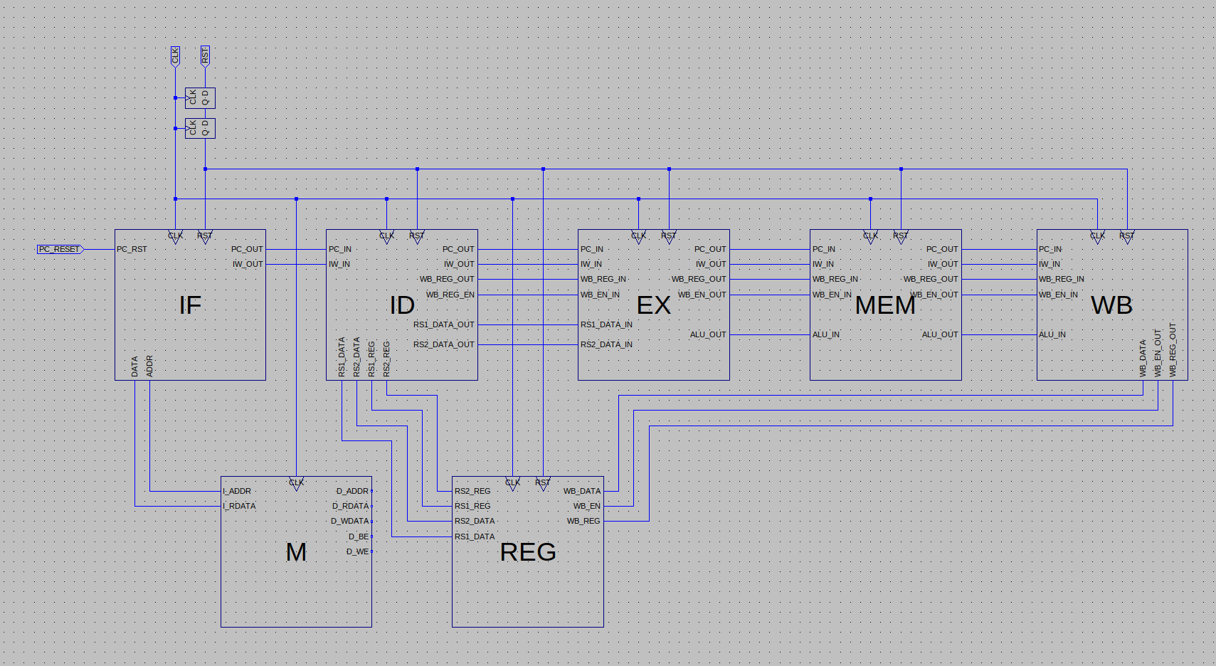
Lab 4: Pipeline Implementation: This lab served to provide the foundational wiring of the
RISC-V pipeline. Most importantly, this portion of the project’s implementation involved the permanent
creation of each of the pipeline’s stages’ top-level files. Establishing the essential wiring and operation
of the pipeline’s stages was essential to add on the additional functionality and features of each of the
stages to be discussed. By the end of this lab’s implementation, we were able to execute instructions in
succession with the processor, so long as there were requisite dummy operations (NOPs) between them. Below is
a loose diagram of the implemented pipeline after this lab’s implementation:
Lab 5: Register Data Forwarding: This lab enabled the operation of register instructions in
succession without the need of NOPs between them. By data-forwarding data from future stages in the
pipeline, our processor’s ID stage was able to send requisite register data to future stages to prevent
register data hazards.
Lab 6: Jump and Branch Logic Implementation: This lab enabled the execution of branch and
jump instructions, which simply alter the program counter’s functionality in the IF stage. This lab also
showcased a flaw in the pipeline, requiring us to stall (send a NOP) to the pipeline when a jump occurs.
This lab majorly altered the implementation of the ID stage to allow for this branching functionality.
Lab 7: Memory Pipeline Implementation: This lab allowed for the programs run on the processor
to finally use load and store instructions, interacting with the processor’s memory as needed. Most simply,
this lab enabled the usage of Lab 3’s Memory Implementation in the processor’s overall pipeline. Note that
a prominent issue in this stage in the processor’s implementation is that memory data hazards exist. These
hazards will be answered by the eigth and final lab:
Lab 8: Memory Data Forwarding: This lab enabled the execution of memory stores and loads
without the need of NOPs between them. This lab involved the creation of stall logic and the data
forwarding of data from the WB stage to the EX stage in order to optimize the speed of the processor.
Additionally, some more data-forwarding was added to the EX stage in order to operate on the most
up-to-date register values in EX, avoiding the need for the ID stage to act upon the inputted rs1/rs2
data values.
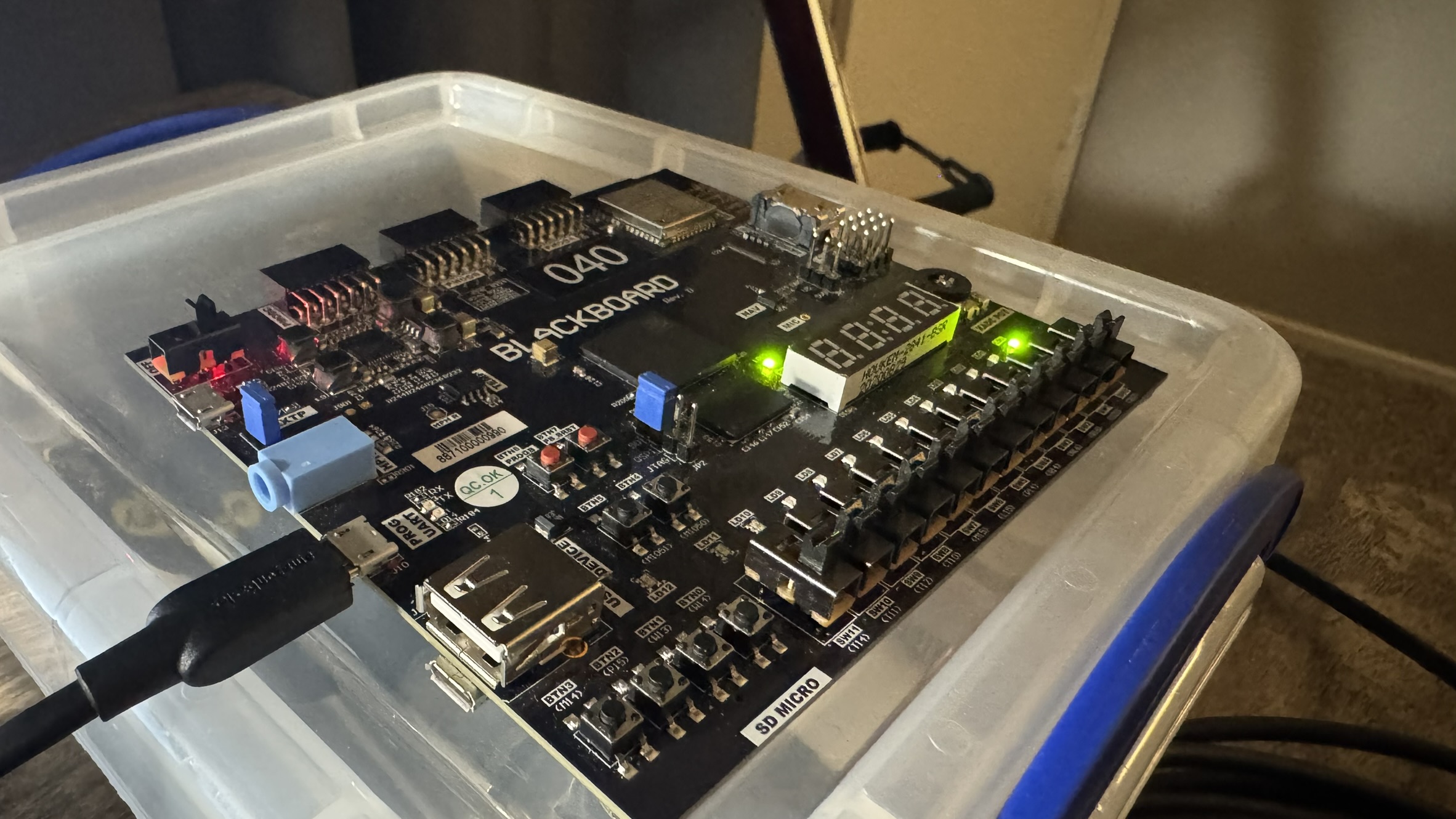
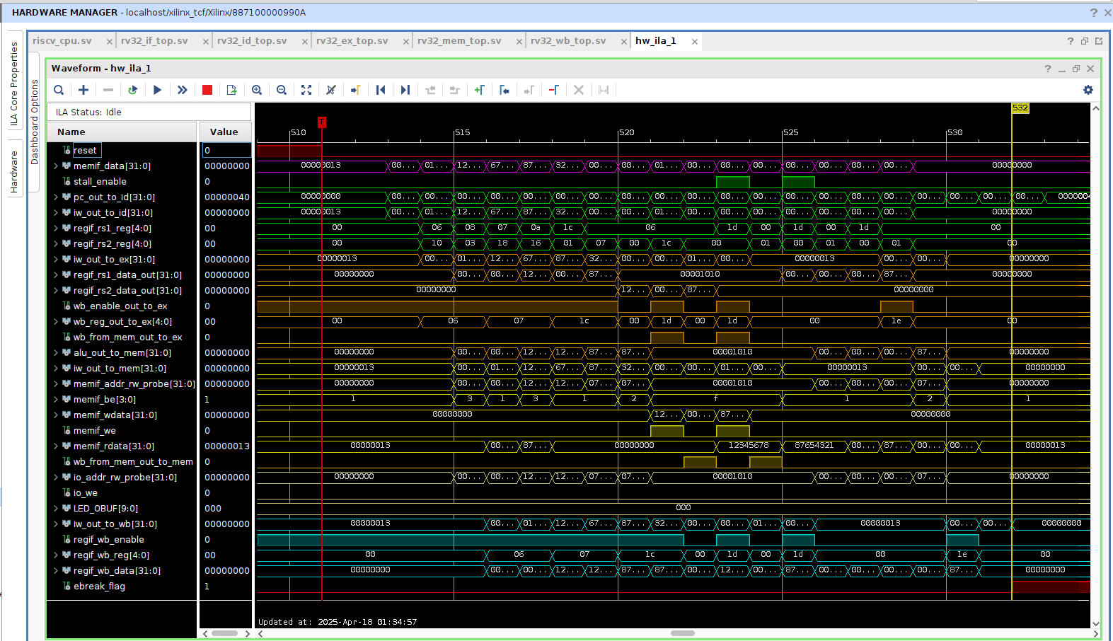
With the completion of this final lab, the RISC-V processor is in a state in which the majority of Assembly
and C programs can be run on it by altering the initial state of the processor’s RAM, loading various
programs upon it. The following photos showcase the processor running a requisite program (flash.s) and
a sample of the ILA for my implementation of the RISC-V processor.
The creation of this RISC-V processor has allowed me to better understand the
functionality of a computer’s processor, and the various ways in which the
pipeline operates upon it. In addition to being an extremely good exercise in
SystemVerilog programming, this project has enabled my understanding of the
creation of processor design utilized in modern-day systems.